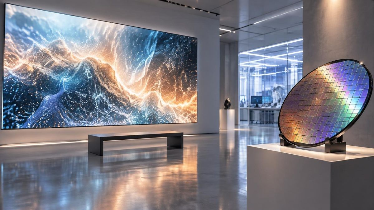
Samsung Electronics is currently advancing its presence in both the consumer design space and the semiconductor manufacturing industry. The company recently detailed new initiatives ranging from artificial intelligence-driven art exhibitions in South Korea to a significant technical partnership with ASML in the Netherlands. These developments highlight the manufacturer's dual focus on aesthetic brand positioning and long-term hardware infrastructure.
Samsung Showcases 'Design Is an Act of Love' at Design Miami Seoul
In the consumer electronics sector, Samsung is hosting an exhibition titled "Design is an Act of Love" at Design Miami Seoul 2026. The event, held at the Dongdaemun Design Plaza (DDP) from September 1 to 6, features 14 Korean artists who have reinterpreted Samsung products using generative AI as a primary creative tool. This exhibition serves as a platform to demonstrate how the company integrates artificial intelligence into the creative process for its latest hardware.
The exhibition highlights several upcoming and current devices, including the Galaxy Z Fold 8 and the Bespoke AI Refrigerator Family Hub. A central component of the display is the OLED TV S95H, which utilizes a "Float Layer Design." This design choice employs a real-metal plate to make the screen appear as if it is hovering. To complement the digital art on display, the S95H is presented with 14 custom frames specifically designed to match the on-screen visuals.
According to Mauro Porcini, President and Chief Design Officer of the Device eXperience (DX) Division at Samsung Electronics, the exhibition reflects a design philosophy centered on human understanding. Porcini stated that while creativity begins with people, AI serves to amplify imagination and extend ideas further. The showcase also features the Music Studio 5, positioning Samsung’s audio equipment alongside its mobile and home appliance categories in a high-design context.
Beyond the artistic applications of its products, the company is also making waves with the underlying technology that powers these devices.
Strategic Collaboration with ASML for Next-Generation Chips
On a different front, Samsung Electronics is expanding its strategic partnership with ASML to advance semiconductor manufacturing. The two companies are focusing on High NA EUV (Extreme Ultraviolet) lithography, a technology critical for producing the next generation of smaller, more efficient chips.
A key technical shift in this partnership involves the transition from 6-inch to 12-inch photomask technology. Samsung is joining an industry initiative to adopt these larger masks, which are expected to provide several manufacturing benefits:
- Increased fabrication plant productivity.
- Reduction in overall chipmaking costs.
- Removal of stitching constraints that currently limit chip design sizes.
Samsung has announced plans to integrate ASML’s High NA EUV lithography into DRAM high-volume manufacturing by 2028. This move is intended to extend the DRAM scaling roadmap by improving resolution and simplifying complex manufacturing steps. By adopting this technology, Samsung aims to provide the hardware foundation necessary for future AI and semiconductor innovation, ensuring that its memory chips can handle the increasing data demands of modern computing.
These two developments illustrate Samsung's current strategy of balancing consumer-facing design with heavy investment in manufacturing infrastructure. While the Seoul exhibition attempts to humanize technology through art and AI, the partnership with ASML ensures the company maintains the technical capacity to produce the high-performance hardware required for those same AI applications. The success of the 2028 DRAM rollout will likely determine Samsung's ability to compete in the high-end semiconductor market for the next decade.